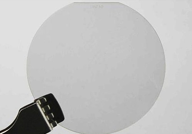
GaN on Sapphire Wafer
GaN Epitxial template on sapphire
Orientation:C-plane(0001)
Film thickness: 0.5~6μm
Diameter: 150.0 ± 0.25mm
Edge exclusion :<4mm
Useable surface area:> 90%
Conduction Type:N-Type
Resisitivity:<0.5Ohm.cm
Carrier Concentration:~1E19 /cc
Macro Defect:≤ 10 / cm-2
Dislocation Density:< 5E8 / cm2
FWHM of RC for the symmetric (002) reflection:~ 250 arcsec
FWHM of RC for the symmetric (102) reflection:~ 300 arcsec
Surface Finish / Polish "RMS <0.5nm by AFM 10μmX10μm scan"
As -Grown:Ga Face
Substrate Sapphire:(0001) miscut 0.2 deg ± 0.1 deg toward M plane
Thickness of Sapphire:"1000μm ± 25μm"
TTV: ≤ 20μm
BOW:≤ 20μm
Warp:≤ 20μm
Polish One side polished (1sp) with the condition of backsurface is "as-received"