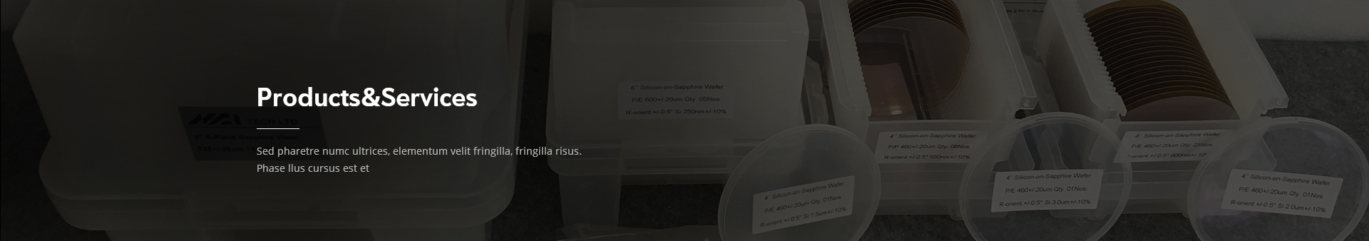
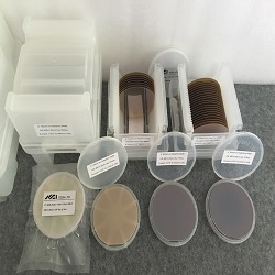
8'' Silicon-on-Sapphire Wafer,Prime grade
Substrate:
Material: 99.996% high purity monocrystalline Al2O3
Orientation: R-Plane (1-102)
Off-cut Non Off-cut: +/- 1.0 degree
Diameter: 200.0 +/- 0.25mm
Thickness: 725 +/- 25 microns
Notch per SEMI M1-1105
Notch location: 45 +/- 2° CCW off C-axis projection onto R-plane
Front Surface: Finish EPI ready polished Ra </= 0.3 nm
TTV: </= 20 microns / Bow: </= 30 microns / Warp: </= 40 microns
Flatness (TIR): </= 20 microns
Back Surface: Fine ground,Ra<1.0um
Laser Marking: Back Side
Packaging: Atmosphere Argon vacuum packed in class 100 clean room
Additional Notes:
Metallic Contamination: <5E10 atoms/cm^2 by VPD for Ca, Na, K, Cr, Zn, Fe, Cu and Ni
LPD: </=40 @ >/=0.2 microns
Edge Exclusion: 5 mm
EPI Layer
Thickness of Silicon EPI Layer center point: 0.1~3.0um +/- 10%
Film Crystallinity & Surface Quality: in accordance with SEMI M4-1296
Resistivity: > 100 Ohm-cm (intrinsic silicon) ; <100 Ohm.cm based on P/N-type doped
Microparticulate density (for particles greater than 2 microns);< 2 per cm^-2